Պատկեր:Cmos-chip structure in 2000s (en).svg

Սկզբնական նիշք (SVG-նիշք, անվանապես 550 × 810 փիքսել, նիշքի չափը՝ 138 ԿԲ)
Ամփոփում
| Նկարագրում |
Català: Estructura esquemàtica d'un xip CMOS, tal com es va construir a principis dels anys 2000. El gràfic mostra els LDD-MISFET sobre un substrat de silici SOI amb cinc capes de metal·lització i un tap de soldadura per a la unió de xip. També mostra la secció per a FEOL (front-end de línia), BEOL (back-end de línia) i les primeres parts del procés de back-end. (versió traduïda a l'alemany)
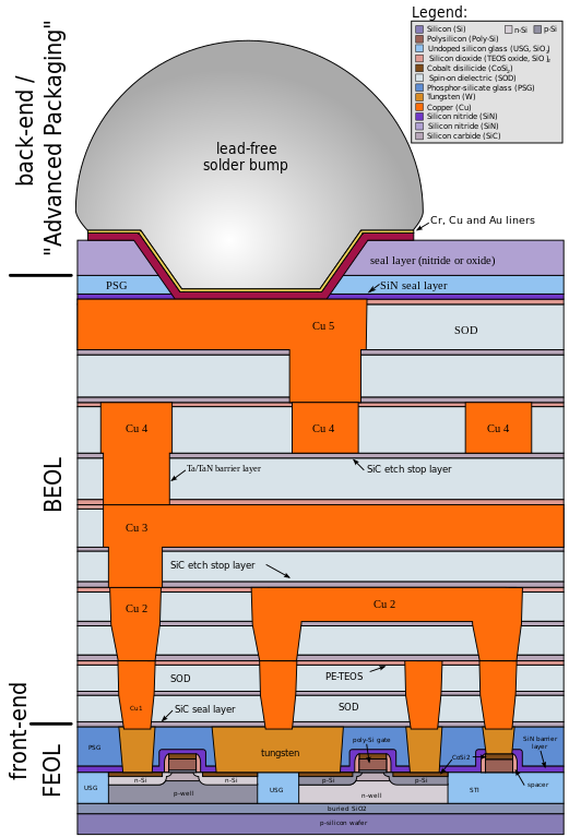
English: Schematic structure of a CMOS chip, like it is built in the early 2000s. The graphic shows LDD-MISFET's on a SOI silicon substrate with five metallization layers and solder bump for flip-chip bonding. Also it shows the section for FEOL (front-end of line), BEOL (back-end of line) and first parts of back-end process. (translated German version) |
| Թվական | 9 Դեկտեմբեր 2006 (upload date) |
| Աղբյուր | self made (from university scripts and scientific papers) |
| Հեղինակ | Cepheiden |
| Այլ մեկնակերպներ |
Other related versions:[]
|
.svg&lang=ca)
.svg&lang=en)

.svg)
.svg)
.svg)
|
Այս SVG ֆայլ օգտագործում է զետեղված տեքստ, որը կարելի է հեշտ թարգմանել ձեր լեզվի վրա using [toolforge:svgtranslate/File:Cmos-chip_structure_in_2000s_(en).svglink this automated tool]: Իմացեք ավելին: You can also download it and translate it manually using a text editor. |
This file is translated using SVG For most Wikipedia projects, you can embed the file normally (without a To translate the text into your language, you can use the SVG Translate tool. Alternatively, you can download the file to your computer, add your translations using whatever software you're familiar with, and re-upload it with the same name. You will find help in Graphics Lab if you're not sure how to do this. |
.svg)
Արտոնագրում

|
Այս վավերագրման պատճենահանման, տարածման և/կամ ձևափոխման թույլտվություն կամ լիցենզիայի GNU FDL պայմաններով 1.2 մեկնակերպի կամ ավելի ուշ, հրատարակված Ազատ ծրագրային ապահովության հիմնադրամում, առանց անփոփոխելի հատվածների, առանց բնագիրների, որոնք տեղադրված են առաջին և վերջին շապիկներում: Լիցենզիայի պատճենը գտնվում է GNU Free Documentation License հատվածում: |
| Այս նիշքը հասանելի է Creative Commons Attribution-Share Alike 3.0 Unported արտոնագրի ներքո: | ||
| ||
| Այս արտոնգրության հատկանիշը ավելացված է տվյալ նիշքին որպես GFDL արտոնագրի բարեփոխում: |
- Դուք ազատ եք՝
- կիսվել ստեղծագործությամբ – պատճենել, տարածել և փոխանցել այս աշխատանքը։
- վերափոխել – ադապտացնել աշխատանքը
- Պահպանելով հետևյալ պայմանները'
- հղում – Դուք պետք է նշեք հեղինակի (իրավատիրոջ) հղումը:
Նիշքի պատմություն
Մատնահարեք օրվան/ժամին՝ նիշքի այդ պահին տեսքը դիտելու համար։
| Օր/Ժամ | Մանրապատկեր | Օբյեկտի չափը | Մասնակից | Մեկնաբանություն | |
|---|---|---|---|---|---|
| ընթացիկ | 14:35, 5 փետրվարի 2024 | | 550 × 810 (138 ԿԲ) | Manlleus | File uploaded using svgtranslate tool (https://svgtranslate.toolforge.org/). Added translation for ca. |
| 14:25, 5 փետրվարի 2024 |  | 550 × 810 (97 ԿԲ) | Manlleus | fixed text labels for translation | |
| 18:52, 9 Դեկտեմբերի 2006 |  | 550 × 810 (85 ԿԲ) | Cepheiden | {{Information |Description= Schematic structure of a CMOS chip, like it is build in the early 2000s. The grafic shows LDD-MISFET's on a SOI silicon substrate with five metallization layers and solder bump for flip-chip bonding. Also it shows the section f | |
| 18:49, 9 Դեկտեմբերի 2006 |  | 550 × 810 (85 ԿԲ) | Cepheiden | {{Information |Description= Schematic structure of a CMOS chip, like it is build in the early 2000s. The grafic shows LDD-MISFET's on a SOI silicon substrate with five metallization layers and solder bumb for flip-chip bonding. Also it shows the section f |
Նիշքի օգտագործում
Հետևյալ էջը հղվում է այս նիշքին՝
Նիշքի համընդհանուր օգտագործում
Հետևյալ այլ վիքիները օգտագործում են այս նիշքը՝
- Օգտագործումը ar.wikipedia.org կայքում
- Օգտագործումը ca.wikipedia.org կայքում
- Օգտագործումը en.wikipedia.org կայքում
- Օգտագործումը fa.wikipedia.org կայքում
- Օգտագործումը fi.wikipedia.org կայքում
- Օգտագործումը ja.wikipedia.org կայքում
- Օգտագործումը ko.wikipedia.org կայքում
- Օգտագործումը zh.wikipedia.org կայքում
.svg)